


In recent years, the pace of miniaturisation of components manufactured in the micro-electro-mechanical systems and nano-electronics sectors has reached unprecedented levels. For efficient development in areas such as biomechanics, transplantology, the space sector or the autonomous vehicle industry, reducing the mass and increasing the strength of components has never been more important. In addition, the use of standard materials and existing processing methods has in many cases pushed us to the limits of technological possibilities. As a result, new materials, often composites where the choice of constituents can influence the physicochemical properties of the final product, and new methods of creating and processing materials are beginning to play a significant role.
The most desired properties of products in modern sectors are low mass, high electrical conductivity and a minimum coefficient of linear expansion of the product walls. These requirements present a number of challenges for research and technology companies, which often have to create entirely new technologies or use existing ones in ways never before seen.
The following article provides an overview and potential applications for the process of creating elements by electrolytic deposition of material onto pre-prepared moulds.
Electroforming, or electroplating as we will focus on here, is not a new idea, but its current applications allow us to address many of the challenges mentioned above. The experience of the team and the unique know-how developed over the years have enabled the development of a unique process for the production of elements with extremely small dimensions, very high precision and controlled physico-chemical parameters. For more details, we invite you to read the rest of the article.
Electroforming: technology description
Electroforming belongs to the field of nanotechnology and allows the controlled growth of multilayer metal structures and metal-carbon nanocomposites, which (depending on the designer’s requirements) can have physicochemical properties different from those of standard alloys and metals. To date, our team has created electroplated products using metals such as Au, Ag, Pd, Cu, Ni, Cr, Ti, Fe or their alloys, and using allotropes of carbon.
The uniqueness of this technology lies in the ability to precisely control the shape and layer structure of the resulting elements. This makes it possible to achieve exceptional surface parameters and a structure free from internal stresses, voids and defects. Importantly, despite the ability to produce elements composed of different metals, these materials should not be considered alloys, as the layered structure achieved by electroforming is significantly different from the structure of metal alloys. The composite (layered) structure and the way in which it is achieved (in other words, the way in which the layers are deposited) directly influence the physico-chemical properties of the final element.
Most interestingly, they can differ significantly from the properties of the individual raw materials and also from the properties of products made by standard metallurgical or galvanic processes.
Electroplating makes it possible to produce parts, devices and systems with parameters that cannot be achieved using other known technologies. It also offers the possibility of solving or circumventing a number of problems faced by engineers and designers working on 5G telecommunications systems, aerospace systems or energy and medical systems.
The unique capabilities of the technology also offer hope for the development of new industries related to the manufacture of electronic and optical systems. Below we present a series of characteristics of electroplating and its advantages over other technologies.
- One of the main advantages of electroplating is the ability to control the physico-chemical properties of the elements produced. This effect is primarily due to the ability to grow the crystallographic lattice of metals precisely and in an ordered fashion and to incorporate other nanoparticles, such as allotropes of carbon, with an accuracy of around 10 nm.
- The limits on the overall dimensions of the elements produced are essentially determined by the dimensions of the reaction chamber used.
- The chemical resistance of the elements produced in an aggressive environment (wet vapours of chlorine, fluorine, etc.) is almost ten times greater than that of the metals deposited by electroplating.
- The hardness of the electroplated composite reaches 20-50 on the Rockwell scale, comparable to the best alloys. The hardness of the surface layer, up to 100 microns thick, reaches the limits characteristic of single crystals. By way of comparison, all currently known additive processes for creating metal elements produce a metal hardness of no more than 5-10 units on the Rockwell scale.
- The structures created are designed computationally, ensuring continuity between the design and manufacturing processes and enabling exceptional precision to be achieved in the production of complex shapes and internal and external surfaces with a designed spatial distribution of the material’s chemical constituents.
- The ability to ‘programme’ the chemical composition and arrangement of atoms and layers of carbon nanoparticles effectively addresses the phenomena of metal fatigue. In addition, the possibility of introducing atoms of certain rare earth metals makes it possible to achieve high strength parameters.
The combination of all the advantages described for electroforming makes it possible to produce materials and products whose quality and parameters significantly exceed those produced by other methods, a fact confirmed by scientific research.
An additional advantage of the electroforming process itself (not directly related to the product being manufactured) is the use of reusable moulds in production. This approach allows mass production of an almost unlimited number of inexpensive, identical products from a single model. High repeatability is maintained, with each element maintaining consistent high quality parameters, including surface finish accuracy.
Products with metal optics, such as flat and curved metal mirrors with complex surface topologies, lenses, prisms, diffraction gratings and components that require exceptionally expensive and precise machining equipment, long production times and considerable physical labour, can be created and replicated in the required quantities at relatively low cost and time.
It’s also important to note that the proposed technology significantly reduces the cost of the production process for elements that require extremely high precision and are manufactured manually using extremely expensive equipment. Replacing the manual process with a repeatable electroforming process not only reduces costs but also increases product repeatability. A prime example is the forming of titanium, which is notoriously difficult to process. The use of an additive process in the manufacture of titanium components completely eliminates the aforementioned manufacturing issues.
Areas of application for electroplating
Applications for electroplating have been identified primarily in microwave electronics, including terahertz technology, optics, quantum electronics, aerospace and the energy sector.
A particularly important practical application could be the production of precise metal optical components, laser reflectors and autocollimators, for example in the manufacture of space navigation systems.
Another practical example of the exceptional accuracy of electroplating is the production of holographic markers. Such a system guarantees very high quality “holographic flare” due to its exceptional manufacturing precision and the absence of random surface defects. The elements contain hidden markers whose ‘flare’ uniquely identifies a particular series of the component. When holograms are created from an imperfect original, the copy will be completely identical to the original, including all random defects.
This repeatable randomness greatly enhances the protective functions of holograms in high volume end products, exceeding the highest security standards at low production costs. Such holograms can have a significant impact on the level of security in the circulation of goods, securities, banknotes, etc.
Electroplating is also used in the production of complex moulds and tools used in the manufacture of plastic components. A mould could be used to produce compact discs or car reflectors, with production time measured in days rather than weeks or months.
The technology can also be used to produce unique, high-quality implantable bioprostheses and implants with a high affinity to the body’s organic tissues. This effect is achieved by incorporating carbon atoms and other elements into the surface layer.
Electroforming also enables unprecedented effects in the production of diffraction gratings operating in the optical and sub-millimetre range. Existing methods of producing these gratings are time-consuming and costly, and it is virtually impossible to produce two identical gratings. The probability of creating identical gratings does not exceed 1×10^-7. Electroplating also allows the creation of hybrid systems consisting of integrated hologram elements, diffraction gratings, resonant elements and optical components.
The long list of producible items also includes integrated microwave systems, parabolic and tubular antennas, laser reflectors, metal optical components, fibre optic elements, microwave absorbers, foamed metals, vacuum lamp components operating in the UHF and THz range, autocollimators and many others.
Electroforming applications in the manufacture of biological implants
Modern medical developments have brought us closer to the widespread use of biological implants to replace damaged tissue and to create implantable components that connect to external mechanical, electronic or computerised systems.
The manufacture of components for this application requires a complex composition, a biologically inert material and a specific, accurately reproduced implant surface topology, shape and structure.
Some orthopaedic applications require a metallic, porous structure with integrated polymer fibres that allow the organism to initiate the process of osteosynthesis and coupling with the implant material of the bone itself, and thus integrate with tendons, muscles and other tissues.
Since each body has its own individual differences in bone structure, it is necessary to create an implant with a well-defined shape. Galvanoplasty is essential for this type of solution, as it allows the creation of products of any highly complex structure.
In addition, the process allows atoms of any material, including non-metals such as carbon, to be incorporated into the structure of the product. An implant with embedded carbon atoms has an increased affinity for body tissues and reduces the risk of rejection and the formation of blood clots on its surface.
The accuracy of 10nm allows for the broad application of electroforming in dentistry, plastic surgery, orthopedics, general surgery, prosthetics, and the creation of artificially controlled limbs.
Examples of metal-carbon nanocomposites obtained through electroforming.
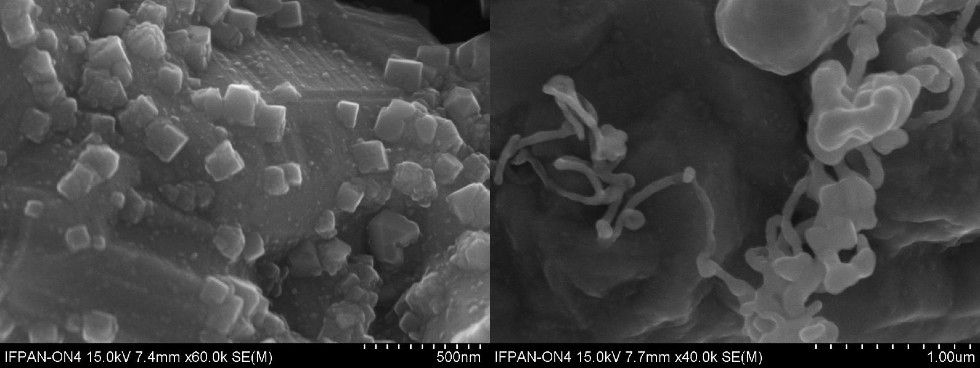
Photo 1, 2 – Copper-carbon nanocomposite
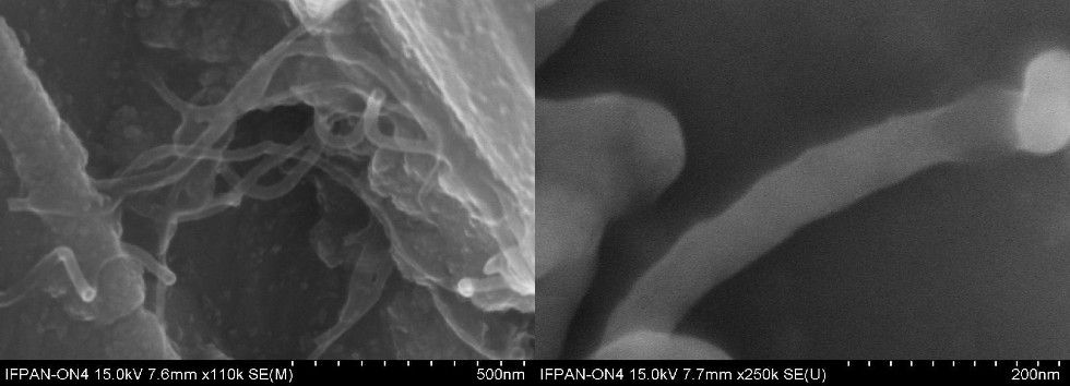
Photo 3, 4 – Nickel carbon nanocomposite
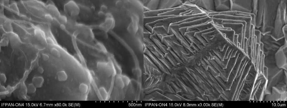
Photo 5, 6 – Nickel – copper – carbon nanocomposite

Gold plated conical antenna for 170-260 GHz frequency range

A generator on a Gunn diode connected to a two-cascade amplifier on an IMPATT diode, containing four T-shaped three-armed circulators

Microwave integrated generator with antenna at 42 GHz + array / microwave waveguide at 140 GHz

Gunn diode generator at 42 GHz


